

26 September 2026
A board for the car, and the 12 V that wants to kill it
How I designed a dedicated Raspberry Pi Pico 2 W board for my Golf IV: why the 12 V input has four protection stages and how I ended up with two TPS54360 converters. The schematic and layout are generated by Python scripts. Revision 0.1, not ordered yet.
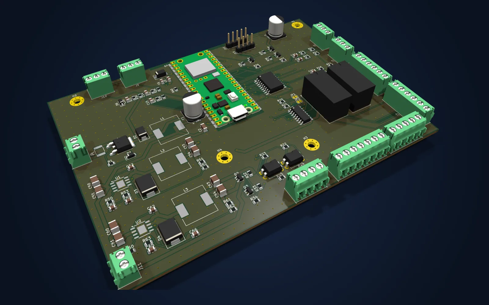
The electronics in my Golf IV are currently a Raspberry Pi Zero 2 W plus a handful of modules on flying leads: a UPS, an ADC, ULN drivers and a separate 12 V charger. That's a lot of connections, and nothing protects the supply from the car's wiring against surges. The current setup stays in the car for now, but I've already designed the board that will replace it, built around a Raspberry Pi Pico 2 W, so that moving over later doesn't turn into a bodge. To be clear from the start: this is revision 0.1 and I haven't ordered it yet. What follows is the design and the decisions that led to it, not a working unit.
Why the Pico 2 W
The Pico 2 W pairs an RP2350, with 520 KB of SRAM and 4 MB of flash, with a CYW43439 radio for Wi-Fi and Bluetooth LE. I went for the version without pin headers, which is soldered flat onto the board by its castellated edges, because it should cope better with vibration. That choice shortened the module list straight away. The UPS was no longer needed, because the Pico boots in under a second and its LittleFS file system survives a sudden power loss. The separate ADC went too, because the RP2350 has its own.
I don't know yet whether the Pico can handle Bluetooth in two roles at once plus TLS 1.3 over PPP. I didn't want the whole design to hinge on that answer, so the board keeps an unpopulated UART header for a Pi Zero 2 W. If the Pico falls short, the Pi sits alongside and the board stays as it is.
What the 12 V input has to survive
A car's electrical system is nothing like a bench supply. The worst of it is load dump, the surge you get when the battery is suddenly disconnected while the alternator is charging. Then there are wires connected the wrong way round. So I laid the protection out as four stages the supply passes through before it reaches the converters. This is that section of the script that generates the schematic:
place('F1', 'Device:Polyfuse', '3A/33V 1812', X + 20, Y, {'1': '+12V_IN', '2': '+12V_F0'}, FP['PTC'])
place('Q1', 'Transistor_FET:Q_PMOS_GSD', 'SQD50P06-15L (-60V)', X + 50, Y,
      {'1': 'Q1_G', '2': '+12V_P', '3': '+12V_F0'}, FP['DPAK'])
place('D1', 'Device:D_Zener', 'BZT52C15 (15V)', X + 45, Y + 20, {'1': '+12V_P', '2': 'Q1_G'}, FP['SOD'])
place('D2', 'Device:D_TVS', 'SMBJ24A', X + 60, Y + 20, {'1': '+12V_P', '2': 'GND'}, FP['SMB'])
place('L1', 'Device:L', '10uH 4A', X + 85, Y, {'1': '+12V_P', '2': '+12V_F'}, FP['L12'])
It starts with a 3 A / 33 V polymer fuse, backed up by an ordinary 5 A fuse in the wiring harness. After the fuse comes reverse-polarity protection on an SQD50P06-15L P-MOSFET (−60 V drain–source) with a 15 V Zener on its gate. Load-dump surges are taken by an SMBJ24A TVS diode. An LC filter finishes the job: a 10 µH, 4 A inductor with 100 µF 50 V and 1 µF capacitors.
How I got to the TPS54360
During load dump the TVS diode clamps at about 39 V, and that's what the converter input may see. That one number drove the whole choice. The first draft used an LM2596 rated to 40 V, which leaves almost no margin at 39 V. For a while the LMR33630 looked like the option with more headroom, but on checking it only goes to 36 V, so that was out as well. On 25 September I switched to the TPS54360, rated to 60 V in, and put two of them on the board.
Two, because the LED strip and the logic shouldn't share a supply. Converter A feeds the Pico (through an SS34 Schottky diode into VSYS), the current sensors and the modem. Converter B feeds only the strip, so a current spike from the strip can't drag the logic rail down. Both deliver 5 V at up to 3.5 A and switch at about 600 kHz. I didn't calculate the component values from scratch; they come from the example in TI's datasheet: an 8.2 µH inductor and a B560C diode.
The strip gets its power through a high-side switch on an AO3401A P-MOSFET under the Pico's control. During a long stop the strip is cut off completely and draws nothing from the battery. The modem has its own identical switch.
Door lock inputs
The Golf IV's factory locks give four signals: latch position and door state, for the driver's and the passenger's side. The lock contact pulls the line to chassis ground, and there is no 12 V on these wires. On the board each line got a 2.2 kΩ pull-up to 3.3 V, a 10 kΩ series resistor to the pin and a 100 nF capacitor. The time constant comes out at about 1 ms, which is enough to swallow spikes from the lock motors. The same 10 kΩ resistor limits the current into the protection diodes during a transient, and firmware debouncing (50 ms) handles the rest.
Windows, mirrors, lock
The windows and mirrors are driven by ULN2803A and ULN2003A Darlington arrays wired in parallel with the factory buttons, so the board 'presses' them just as the driver would. The common COM pin goes to 12 V after the protection stage, which lets the flyback diodes built into the chips do their job.
One detail I took from the errata. The RP2350 has a documented issue, E9, affecting its internal pull-down resistors, so I don't rely on them. The ULN inputs have their own resistors to ground, and the transistor bases, optocouplers and relay inputs get external 100 kΩ pull-downs. As a result, after a reset and before the firmware has set up its pins, no output is 'pressed', so no window moves and no remote button is pushed.
I handled the central lock the same way as in the Pi design: two PC817 optocouplers press the buttons of a spare remote with a 400 ms pulse, and the remote stays galvanically isolated from the board. I also left footprints for two Omron G5V-2 relays to reverse the polarity of the mirror motors. They stay unpopulated for now, because I haven't yet checked the car's wiring diagram to see whether the mirror switch needs them.
Schematic and layout from scripts
Nothing here was drawn by hand. The circuit is described in a script, gen_sch.py, and that file is the source of truth: it generates the KiCad schematic with a net label on every pin, while the design decisions are written up separately in the spec. kicad-cli then exports the netlist from the schematic. A second script, run in KiCad's own Python, builds the board from it: it places the parts from a dictionary of positions and adds the outline, net classes, the antenna keep-out and the ground pours. Freerouting then routes the traces (20 passes take about ten minutes), and a final script adds the ground-stitching vias. Any change to the spec means rerunning the whole chain. Manual edits in KiCad would be overwritten in the process, so every change has to go into the scripts.
The result is a 140 × 100 mm two-layer board with a ground pour on both sides and 96 parts to populate across 48 BOM lines. Power traces are 1.2 mm wide and signal traces 0.3 mm. The Pico lies at the top edge, turned so that its antenna reaches the board edge with no copper underneath. ERC and DRC report no errors. DRC leaves only cosmetic silkscreen warnings and four Pico ground pads that aren't tied to the pour. I'm fine with that, because the module's internal ground connects all of its ground pins. The manufacturing files are ready: Gerbers, BOM, pick-and-place positions and a STEP model for designing the enclosure in FreeCAD.
What I don't know yet
Before I order boards, a prototype on a bare Pico has to settle the questions that made me add the Pi header. Bluetooth must work in two roles at once: central towards the LED controller and peripheral towards the phone. TLS 1.3 has to run over PPP through the LTE modem, and the WireLink channel on mbedTLS has to match the current gateway's test vectors byte for byte. On the board itself I still need to confirm in Waveshare's documentation that the modem's PWRKEY is triggered by pulling it to ground (that's how it's drawn), and to recalculate the TPS54360 compensation for the 2 × 47 µF output capacitors.
The project write-up is in the portfolio, and you can turn the board around in the interactive 3D model. It comes straight from the KiCad project; click a block to see what it does and what it's made of.